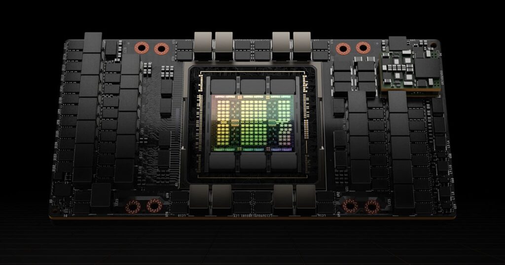
The explosion of Generative AI and massive Large Language Models (LLMs) has fundamentally changed the computing landscape. Behind the magic of tools like ChatGPT and Midjourney lies a foundation of raw, unadulterated computing power. At the bleeding edge of this hardware revolution is the Nvidia H100 Tensor Core GPU.
Built on the groundbreaking Nvidia Hopper architecture, the H100 is not just an iterative upgrade; it is a purpose-built engine designed to accelerate enterprise AI, massive-scale scientific computing, and data center operations.
In this guide, we will dive deep into the Nvidia H100, exploring its core specifications, form factors, and how it stacks up against its predecessor, the A100.
What is the Nvidia H100 GPU?
The Nvidia H100 is an enterprise-grade data center GPU designed to handle the most computationally intensive workloads on the planet. Whether it is training trillion-parameter AI models or running complex climate simulations, the H100 is engineered for unprecedented scale.
The Leap to Hopper Architecture
Replacing the previous Ampere architecture, the Hopper architecture (named after pioneering computer scientist Grace Hopper) introduces a massive leap forward in accelerated computing. Hopper was designed from the ground up to solve the bottlenecks associated with scaling up AI operations across thousands of GPUs, dramatically improving memory bandwidth, interconnect speeds, and computational efficiency.
The Breakthrough Transformer Engine
The standout feature of the H100 is its native Transformer Engine. Transformer models are the backbone of modern LLMs. The H100 uses advanced software and custom Hopper hardware to dynamically choose between 8-bit floating point (FP8) and 16-bit floating point (FP16) calculations. This allows the H100 to speed up AI training by up to 6x compared to the previous generation, all without sacrificing accuracy.
Nvidia H100 Specifications & Key Features
To understand why the H100 commands such a premium in the AI industry, you have to look under the hood. Here are the core specifications that define this powerhouse:
- 4th-Generation Tensor Cores: Delivering matrix computations at breakneck speeds, these new cores drastically reduce the time it takes to train massive AI models.
- HBM3 Memory & Bandwidth: The H100 features up to 80GB of cutting-edge HBM3 memory, delivering a staggering 3.35 TB/sec of memory bandwidth to keep the compute cores constantly fed with data.
- Next-Gen NVLink: Scaling AI requires GPUs to talk to one another instantly. The 4th-generation NVLink provides 900 GB/s of GPU-to-GPU interconnect bandwidth—a 50% increase over the previous generation.
- Multi-Instance GPU (MIG): Not every workload requires an entire H100. Second-generation MIG technology allows a single H100 to be securely partitioned into up to seven distinct instances, allowing multiple users or smaller workloads to share the hardware efficiently.
- DPX Instructions: For dynamic programming algorithms used in genomics, route optimization, and logistics, Hopper’s new DPX instructions deliver up to a 7x performance boost over Ampere GPUs.
Nvidia H100 Form Factors Explained
Data centers have different physical and thermal requirements, which is why Nvidia offers the H100 in distinct form factors:
H100 SXM vs. PCIe
- SXM5 Form Factor: Designed for maximum, uncompromising performance within HGX server boards. The SXM version operates at a massive 700W Thermal Design Power (TDP) and is built for tightly coupled, multi-GPU clusters.
- PCIe Gen 5 Form Factor: A dual-slot card tailored for mainstream enterprise servers. It operates at a lower 350W TDP, making it easier to integrate into existing data center racks while still delivering incredible performance.
H100 NVL
Nvidia also introduced the H100 NVL, a dual-GPU PCIe card connected via an NVLink bridge. Optimized specifically for deploying massive LLMs, the NVL configuration pairs two GPUs to provide a combined 188GB of HBM3 memory, perfectly suited for heavy inference workloads.
Nvidia H100 vs. A100: Is the Upgrade Worth It?
For enterprises holding onto Nvidia A100 clusters, the core question is whether the massive investment in the H100 is justified. The short answer is yes—especially for Generative AI.
The H100 delivers up to 9x faster AI training and up to 30x faster AI inference on Large Language Models compared to the A100. While the H100 draws more peak power (700W vs 400W for SXM), it completes complex workloads so much faster that it ultimately lowers the Total Cost of Ownership (TCO) and energy consumed per workload.
Quick Comparison Table
| Feature | Nvidia H100 (SXM) | Nvidia A100 (SXM) |
| Architecture | Hopper | Ampere |
| Memory | 80GB HBM3 | 80GB HBM2e |
| Memory Bandwidth | 3.35 TB/s | 2 TB/s |
| Tensor Cores | 4th Generation | 3rd Generation |
| NVLink Bandwidth | 900 GB/s | 600 GB/s |
| Max TDP | 700W | 400W |
| Transformer Engine | Yes (Native FP8) | No |
The Nvidia GPU Roadmap: H100 vs. H200 vs. Blackwell
While the H100 remains the industry standard, the AI hardware landscape moves at lightning speed. Nvidia’s H200 GPU builds upon the Hopper architecture by introducing 141GB of faster HBM3e memory, enabling even faster inference for massive LLMs. Looking further ahead, the transition to the Blackwell (B200) architecture represents the next paradigm shift, promising another massive multiplier in compute density and efficiency to train the multi-trillion-parameter models of tomorrow.
Top Use Cases for the Nvidia H100
- Generative AI & LLMs: Training and running inference for foundational models that require massive parallel processing.
- High-Performance Computing (HPC): Accelerating scientific breakthroughs in climate modeling, quantum chemistry, and drug discovery.
- Real-Time Data Analytics: Parsing through massive enterprise datasets instantly to drive business intelligence and predictive modeling.
Conclusion
The Nvidia H100 is the undisputed engine of the AI revolution. By introducing the Hopper architecture, the Transformer Engine, and lightning-fast HBM3 memory, Nvidia has provided the exact hardware the industry needs to push the boundaries of Generative AI and High-Performance Computing.
Frequently Asked Questions
Pricing heavily depends on supply, volume, and vendor relationships, but individual H100 PCIe cards typically range between $30,000 to $40,000 on the enterprise market.
The PCIe version has a peak TDP of 350W, while the higher-performance SXM version consumes up to 700W.
Technically, yes, but it is entirely impractical. The H100 is vastly over-engineered (and overpriced) for cryptocurrency mining. Its true value lies in precision AI calculations, not hashing algorithms.
The H100 is a standalone GPU. The GH200 (Grace Hopper Superchip) combines an Nvidia Grace CPU and a Hopper GPU onto a single board, sharing a massive pool of unified memory to eliminate bottlenecks between the CPU and GPU.
Comments